(China (Mainland))

Product Summary
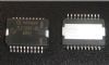
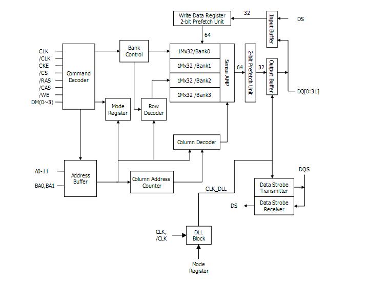
The HY5DU283222AQ-5 is a 134,217,728-bit CMOS Double Data Rate(DDR) Synchronous DRAM, ideally suited for the point-to-point applications which requires high bandwidth. The HY5DU283222AQ-5 offer fully synchronous operations referenced to both rising and falling edges of the clock. While all addresses and control inputs are latched on the rising edges of the CK (falling edges of the /CK), Data, Data strobes and Write data masks inputs are sampled on both rising and falling edges of it. The data paths are internally pipelined and 2-bit prefetched to achieve very high bandwidth. All input and output voltage levels are compatible with SSTL_2.
Parametrics
HY5DU283222AQ-5 absolute maximum ratings: (1)Ambient Temperature:0℃ to 70℃; (2)Storage Temperature:-55℃ to 125℃; (3)Voltage on Any Pin relative to VSS:-0.5V to 3.6V; (4)Voltage on VDD relative to VSS:-0.5V to 3.6V; (5)Voltage on VDDQ relative to VSS:-0.5V to 3.6V; (6)Output Short Circuit Current:50mA; (7)Power Dissipation:1W; (8)Soldering Temperature.Time:260.10 ℃.sec.
Features
HY5DU283222AQ-5 features: (1)VDD, VDDQ = 2.5V ± 5%; (2)All inputs and outputs are compatible with SSTL_2 interface; (3)JEDEC standard 20mm x 14mm 100pin LQFP with 0.65mm pin pitch; (4)Fully differential clock inputs (CK, /CK) operation; (5)Double data rate interface; (6)Source synchronous - data transaction aligned to bidirectional data strobe (DQS); (7)Data outputs on DQS edges when read (edged DQ) Data inputs on DQS centers when write (centered DQ); (8)Data(DQ) and Write masks(DM) latched on the both rising and falling edges of the data strobe; (9)All addresses and control inputs except Data, Data strobes and Data masks latched on the rising edges of the clock; (10)Write mask byte controls by DM (DM0 to DM3); (11)Programmable CAS Latency 3 and 4 supported; (12)Programmable Burst Length 2 / 4 / 8 with both sequential and interleave mode; (13)Internal 4 bank operations with single pulsed RAS; (14)tRAS Lock-Out function supported; (15)Auto refresh and self refresh supported; (16)4096 refresh cycles / 32ms; (17)Half strength and Matched Impedance driver option controlled by EMRS.
Diagrams
 |
 HY5DS113222FM |
Other |
|
Data Sheet |
Negotiable |
|
||||
|
HY5DS283222BF |
Other |
|
Data Sheet |
Negotiable |
|
||||
|
HY5DS283222BFP |
Other |
|
Data Sheet |
Negotiable |
|
||||
|
HY5DS573222F |
Other |
|
Data Sheet |
Negotiable |
|
||||
|
HY5DS573222P |
Other |
|
Data Sheet |
Negotiable |
|
||||
|
HY5DU121622A |
Other |
|
Data Sheet |
Negotiable |
|
||||